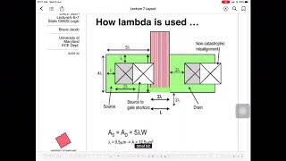
Web Reference: Step-by-step 3-D visualization of fabrication for any portion of layout. In the following, we present a sample set of the lambda-based layout design rules devised for the MOSIS CMOS process and illustrate the implications of these rules Mask design is aimed at turning a specification into masks for processing silicon to meet the specification. Stick Diagrams may be used to convey the layer information through the use of colour code. For Depletion mode transistor, Implant within the thin oxide is a must.
YouTube Excerpt: VLSI
Information Profile Overview
Mask Layout Lambda Based Design - Latest Information & Updates 2026 Information & Biography

Details: $2M - $18M
Salary & Income Sources

Career Highlights & Achievements


Assets, Properties & Investments
This section covers known assets, real estate holdings, luxury vehicles, and investment portfolios. Data is compiled from public records, financial disclosures, and verified media reports.
Last Updated: April 3, 2026
Information Outlook & Future Earnings

Disclaimer: Disclaimer: Information provided here is based on publicly available data, media reports, and online sources. Actual details may vary.